最近,在一篇由英國航空研究所(ATI)和曼切斯特大學國家石墨烯研究院(NGI)聯合發表的論文中,研究人員指出,石墨烯的應用有可能給航空航天領域帶來顛覆性的變革。
2004年,曼切斯特大學的兩名科學家在用膠帶清理一塊石墨晶體時,發現他們在膠帶上分離出了一層碳原子。石墨烯由此誕生。至此以后,石墨烯因其驚人的特性引發了科研界的密切關注。石墨烯的強度是鋼的200倍,不僅具備優異的柔韌性,還是絕佳的導電體。
曼切斯特大學的科研人員表示,這種二維材料有望幫助改善飛行器的性能、降低造價、提高能效。如果在當前的飛行器制造材料中添加只有一個原子厚度的石墨烯,那么飛行器的安全性將顯著增強,其它性能也將明顯改善。如此一來,還能實現機身輕量化和節能環保的目標。
該篇論文發表于ATI的《INSIGHT》期刊,前言由理查德·布蘭森爵士親自撰寫。文中寫道,“石墨烯有望解決航空航天領域中一些由來已久的挑戰,繼而引發行業革命,成為未來航空航天技術發展的關鍵動力。我們需要大力開展石墨烯相關科研技術項目,加深國內對石墨烯優點的認識,為我國航空業的發展做出實質性貢獻。”
石墨烯研發的最新進展
石墨烯近來的迅猛發展讓這一材料成為了關注焦點。
二月,日本東北大學和名古屋大學的科研人員成功研制出兩種新型三層石墨烯。這兩種新材料均由三層石墨烯組成,但堆垛方式和導電性不同。這一成果將推動光電轉換光伏電池等新型電子設備的研發。
石墨烯的碳原子呈六角形蜂巢晶格狀分布,有兩種常見的雙層堆垛方式:一是AA堆垛,即上下兩層緊密重合;二是AB堆垛,即上下兩層之間存在一個碳原子的距離。這兩種堆垛方式目前已成功實現。如果加上外電場,AB堆垛雙層石墨烯便會成為半導體。
相較之下,三層堆垛很難實現。日本科研人員用兩種特殊方法加熱碳化硅,終于成功制備出了兩個三層石墨烯樣品。
科研人員將碳化硅在加壓氬氣和高真空中分別加熱到1510℃和1300℃,再噴上氫氣。氫氣中的氫鍵破裂,形成單層氫原子,最后結合形成三層石墨烯。
在加壓氬氣中加熱的碳化硅呈ABA堆垛,即上下兩層重合,中間層錯開。而在真空下加熱的碳化硅則呈ABC堆垛,即每層稍微錯開。
研究人員在檢測兩個石墨烯樣本的物理性質時,發現兩者的導電性是不同的。
ABA堆垛的樣品和單層石墨烯相似,都是極佳的導電體。而ABC堆垛的性質更接近于AB堆垛雙層,具有半導體特性。
本月,新加坡國立大學的一個科研小組又發明了新的石墨烯制備方法,所用的溶劑量是現行方法的1/50,為大規模、可持續合成打開了大門。
傳統的石墨烯制備方法是利用剪力剝離石墨,再將其置于大量溶劑中,(比例為一千克石墨烯兌近一噸有機溶劑),這就產生了生態可持續性問題。如果減少溶劑,石墨烯層又會重新吸附到石墨上。
新的制備法是在高堿性環境下剝離預處理后的石墨。石墨烯在堿性環境下會發生絮凝,無需增加溶劑就能使石墨烯層聚集形成石墨烯漿料,接著把漿料分離成更常用的單層石墨烯即可。
新制備法通過引進靜電工藝,成功防止了石墨烯片層的重新吸附。此外,石墨烯漿料是一種具有海綿狀結構的超輕材料,也可直接用作3D打印的導電氣凝膠。
前進的道路
曼切斯特大學Graphene@Manchester公司CEO James Baker在評論這篇發表于《INSIGHT》的論文時表示,“航空航天領域的重要進步歷來都是和新材料的應用有關。鋁材和碳纖維讓飛機更快、更環保、成本更低、功能更強大。現在,石墨烯和相關的二維材料將引發下一場變革。”
“在現有的飛機制造材料中加入石墨烯,將改善飛機的許多關鍵性能。多功能石墨烯的應用和產學研合作的加深將為下一代航空技術的加速發展提供契機。”
與此同時,中國和英國也已在石墨烯研發領域建立了深層合作關系。中國目前是最大的石墨烯制造國,英國則是全球石墨烯研發中心。中英兩國的航空業目前都處在關鍵發展時期,英國政府力圖振興歷史悠久的航空業,而中國正在崛起成為全球商業中心和技術高地。
石墨烯顛覆航空航天行業,或將指日可待?
Recent innovations in Japan, Singapore as University of Manchester launches graphene aerospace strategy
In a recent joint paper by the Aerospace Technology Institute (ATI) and the National Graphene Institute (NGI) at the University of Manchester, researchers outlined the disruptive impact potential of graphene applications in aerospace.
The development of graphene dates back to 2004, when two University of Manchester scientists realized they had isolated a single layer of carbon atoms on a piece of scotch tape used to clean a graphite crystal. Since then, graphene has captured the imagination of researchers due to its fascinating properties. It is 200 times stronger than steel, very flexible, and is an excellent conductor of electricity.
According to the Manchester researchers, the two-dimensional material has the potential to positively impact aircraft performance, cost, and fuel efficiency. By incorporating atomically-thin graphene into existing materials used to build aircraft, the safety and performance properties of aircraft could be significantly improved. This in turn, could lead to reduced material weight and positive impact on the fuel efficiency of the aircraft and, as result, the environment.
In an exclusive introduction to the paper (published in ATI’s INSIGHT series), Sir Richard Branson said, “The potential for graphene to solve enduring challenges within the aerospace sector presents real opportunities for the material to become disruptive, and a key enabler in future aircraft technology. We need to accelerate the opportunity for the UK to realize the benefits from graphene by creating a portfolio of graphene-related research and technology projects which if undertaken would lead to real impact in our aerospace industry.”
Recent graphene development
This focus on graphene comes during a period of marked development of the material.
In February, Tohoku University and Nagoya University researchers discovered a way to form two new tri-layer graphene materials. Each of the novel material—both made of three layers of graphene—is layered differently and has unique electrical properties. The work has implications for the development of novel electronic devices, such as photovoltaic cells that convert light into electrical energy.
Graphene's carbon atoms are arranged into hexagons, forming a honeycomb-like lattice. The deliberate bi-layering graphene—either with the centers of the carbon hexagons layered immediately above one another, “AA-stacking,” or the displaced layering with a hexagon center above a carbon atom of the second layer “AB-stacking”—has been achieved successfully in the past. Furthermore, if an external electric field is applied, AB-stacking of two layers of graphene leads to the formation of a material with semiconducting properties.
However, the deliberate stacking three layers of graphene has proven difficult. The Japanese researchers developed a way to fabricate the two tri-layer graphene samples by heating silicon carbide using two distinct methods.
In one experiment, the silicon carbide was heated to 1,510°C under pressurized argon. In another, it was heated to 1,300°C in a high vacuum. Both materials were then sprayed with hydrogen gas in which the bonds were broken to form single hydrogen atoms, forming the tri-layer graphene.
The silicon carbide heated under pressurized argon formed into ABA-stacked graphene, with matching top and bottom hexagon layers sandwiching a displaced middle layer. The silicon carbide heated in a vacuum developed into ABC-stacked graphene, in which each layer was slightly displaced in front of the one below it.
When the researchers examined the physical properties of each material, they found that electrons behaved differently between the two types of graphene samples.
The ABA graphene was an excellent electrical conductor, similar to mono-layer grapheme. However, the ABC graphene, behaved more like AB graphene in that it had semi-conducting properties.
Just this month, a research team from the National University of Singapore developed a new graphene production method requiring 50 times less solvent than current methods, potentially opening the door for larger-scale, sustainable synthesis.
The conventional method for graphene production makes use of shearing forces to lift layers from graphite. These are then dispersed in large volumes of solvent (approximately one ton of organic solvent to one kilogram of graphene), which presents an issue of ecological sustainability. Often, when reducing solvent volume graphene layers reattach to the graphite.
The new method was discovered by exfoliating pre-treated graphite under higher than normal alkaline conditions, which triggers flocculation, prompting the graphene layers to cluster together into a slurry without the need to increase solvent content. The graphene slurry can then be separated into more commonly used monolayers.
The method prevents reattachment to the graphite via a newly introduced electrostatic process. The slurry can also be used directly to 3D-print conductive graphene aerogels, an ultra-lightweight sponge-like material.
The path forward
In a comment published concerning the INSIGHT paper, James Baker, CEO of Graphene@Manchester at the University of Manchester concluded, “Major generational improvements in the aerospace sector have been associated with embracing new materials. Aluminum and carbon fiber have seen planes become faster, greener, cheaper with more functionality. Now graphene and related two-dimensional materials can mark the next step-change.
“By incorporating graphene into the existing materials used to manufacture planes, performance properties could be improved across number of key areas. By utilizing the multi-functional properties of graphene and through collaboration between industry and academia, there are significant opportunities which can accelerate the next-generation of aerospace technologies.”
Furthermore, there is currently heavy cooperation regarding graphene development between Chinese researchers (China is a top producer of graphite) and UK researchers (at epicenter of graphene development). Both countries are in the midst of aerospace development, with the UK working to restore a waning industry full of aviation heritage and China becoming a burgeoning commercial hub and early adopter of new technologies.
How long before the aerospace industry sees the disruptive impact?
Author: William Kucinski
Source: SAE Aerospace Engineering Magazine
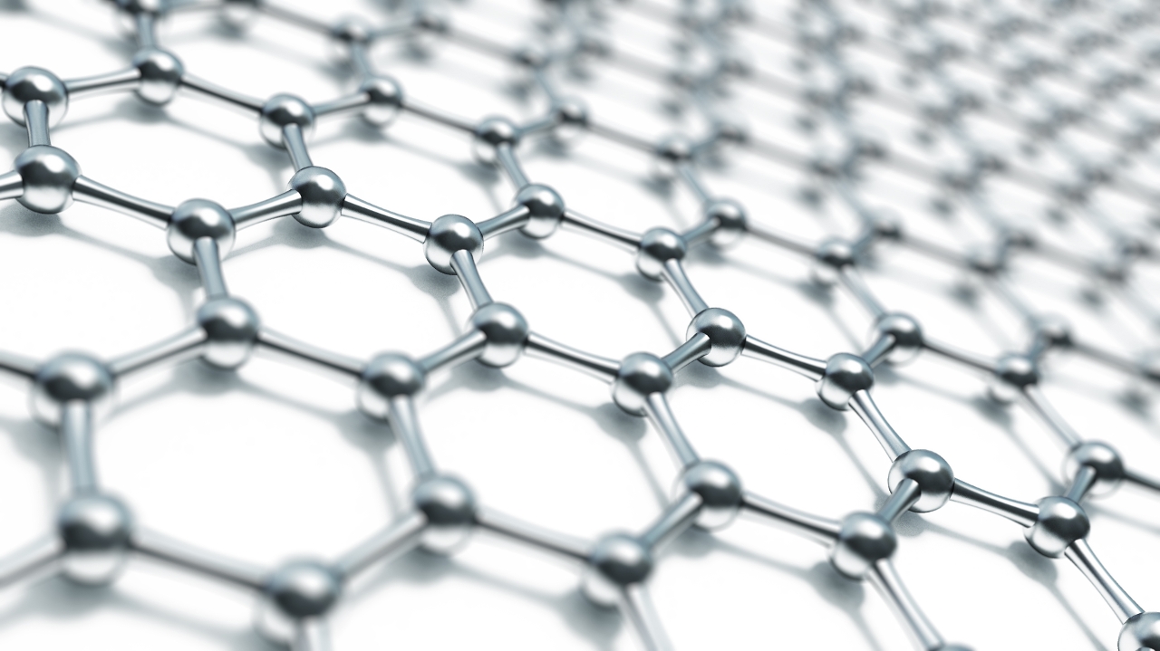 石墨烯因其驚人的特性成為了科研界的關注焦點。石墨烯的強度是鋼的200倍,不僅具備優異的柔韌性,還是絕佳的導電體。研究人員相信石墨烯將引發航空航天領域的材料革命。